This is a collection of pictures of the various stages in the DFA testing at UCSB.
(Click on any image to view a larger GIF version of the picture)
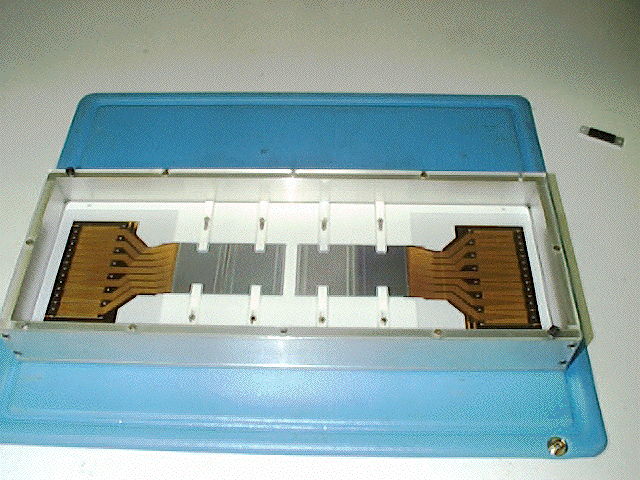
This is a picture of two Layer 2 DFAs (one forward and one backward) in the shipping fixture used by Pisa to deliver the DFAs to UCSB:
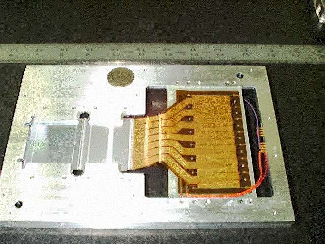
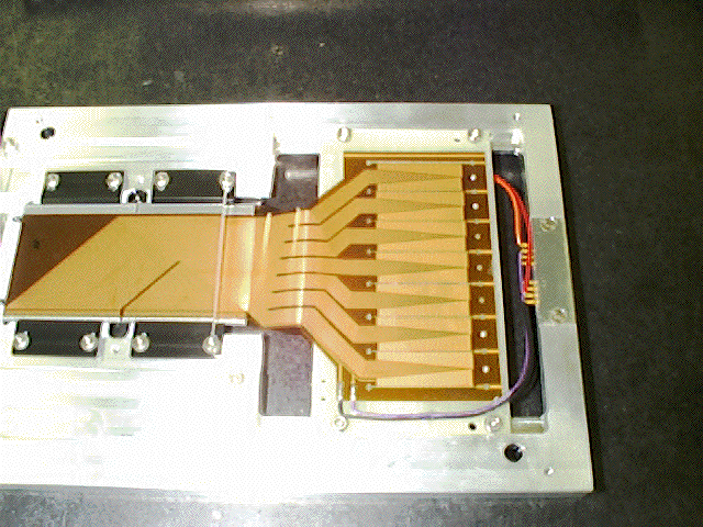
Here are pictures of the Phi and Z side of one of the DFAs after it has been placed in a ring frame fixture.
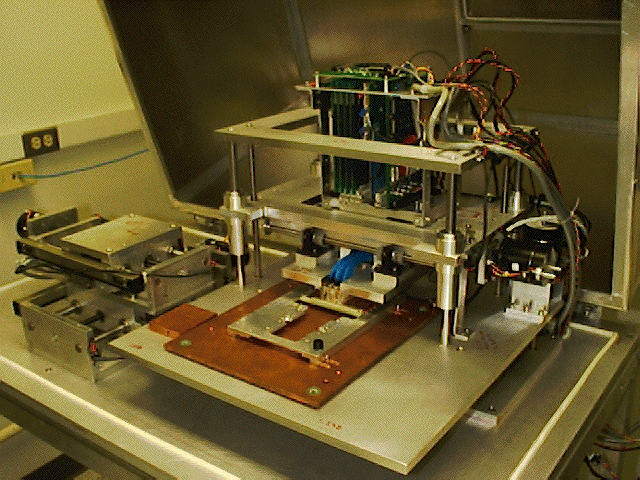
Before the HDI is attached to the DFA, the DFA must be tested using this multichannel DFA testing station. This station is capable of detecting shorts between strips, strips with broken coupling capacitors, and other defects by capacitance and low-level current measurements. The test station will also be used to perform LED scans on the DFA.
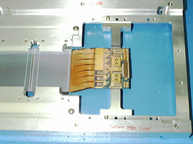
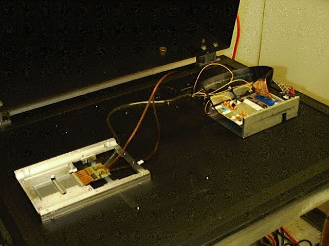
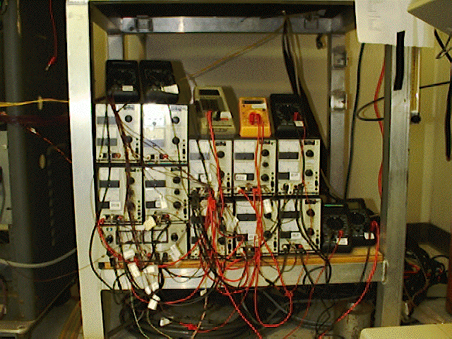
After the DFA has been completely wire bonded and tested, it gets attached to an HDI and tested. Here is a picture of the DFA after it has been attached to a HDI with 3 ICs mounted on each side. The next picture shows this HDI hooked up to a prototype matching card with flexible Kapton tails. The entire system receives it's power from our beautiful array of power supplies.
Comments to roberts@hep.ucsb.edu![]()
File last updated January 24, 1997.